(China (Mainland))

Product Summary
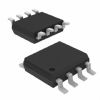
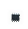
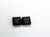
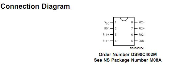
The DS90C402MX is a dual receiver device optimized for high data rate and low power applications. This device along with the DS90C401 provides a pair chip solution for a dual high speed point-to-point interface. The DS90C402MX is in a PCB space saving 8 lead small outline package. The receiver offers ±100 mV threshold sensitivity, in addition to common-mode noise protection.
Parametrics
DS90C402MX absolute maximum ratings: (1)Supply Voltage (VCC): -0.3V to +6V; (2)Input Voltage (RIN+,RIN-): -0.3V to (VCC + 0.3V); (3)Output Voltage (ROUT): -0.3V to (VCC + 0.3V); (4)Maximum Package Power Dissipation @ +25℃: 1025 mW; (5)Derate M Package 8.2 mW/℃: above +25℃; (6)Storage Temperature Range: -65 to +150℃; (7)Lead Temperature Range Soldering (4 sec.): +260℃; (8)Maximum Junction Temperature: +150℃.
Features
DS90C402MX features: (1)Ultra Low Power Dissipation; (2)Operates above 155.5 Mbps; (3)Standard TIA/EIA-644; (4)8 Lead SOIC Package saves PCB space; (5)VCM ±1V center around 1.2V; (6)±100 mV Receiver Sensitivity.
Diagrams
| Image | Part No | Mfg | Description |  |
Pricing (USD) |
Quantity | ||||||||||
|---|---|---|---|---|---|---|---|---|---|---|---|---|---|---|---|---|
 |
 DS90C402MX |
National Semiconductor (TI) |
LVDS Interface IC |
Data Sheet |
|
|
||||||||||
 |
DS90C402MX/NOPB |
National Semiconductor (TI) |
LVDS Interface IC |
Data Sheet |
|
|
||||||||||